Transparent Conductive Films and Materials 2018-2028: Global Forecasts, Technologies, Players
BOSTON, June 29, 2018 (Newswire.com) - The market for transparent conductive films and materials has been rapidly changing. This continuing transformation is taking place at all levels: technologies, applications and suppliers. The recent market report from IDTechEx Research, Transparent Conductive Films and Materials 2018-2028: Forecasts, Technologies, Players, provides the most comprehensive and authoritative view of this industry.
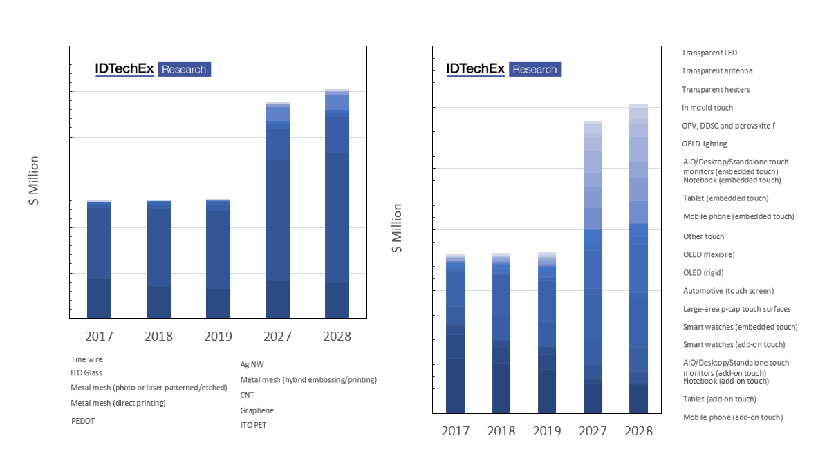
The past: major technology shifts and market changes to date
IDTechEx Research forecasts that the total market for transparent conducting layers (glass and film) will double by 2028 compared to its 2017 value (in the considered applications). The short-term prospect, however, is stagnation. There will be some growth in use cases, but this will be offset by price squeezes. In the medium- to long-term, growth will be fuelled by the emergence of new and/or larger area applications.
Dr Khasha Ghaffarzadeh, Research Director, IDTechEx
Author of the report, IDTechEx Research Director Dr Khasha Ghaffarzadeh, comments: "Technology cycles are often short-lived in consumer electronic markets. Touch displays are also no exception. Indeed, we have witnessed many sweeping changes since 2008, the time when IDTechEx Research started analysing this market.
Within the years that IDTechEx Research has been covering the TCF market, we witnessed the rise of p-cap technology which essentially rendered resistive touch obsolete. In more recent years, we witnessed the rise of embedded (vs. add-on) touch technology, shifting the value from panel to displays makers and adversely affecting the addressable market for film supply.
In parallel to these technology shifts, the market composition of touch display technology also changed. Mobile phones exited the period of rapid unit sale growth whilst low-cost challenger companies appeared in emerging markets. Tablets first grew in sales but then reversed the trends, entering a period of sustained decline. Notebook sales stabilized but touch technology did not penetrate as rapidly as others had hoped whilst All-in-Ones generally undershot original industry expectations.
Numerous non-touch markets were also in development mode. In the main however, these failed to grow out of the nascent states. The limitation was rarely the transparent conductor technology. Instead, these emerging technologies were often faced with a mighty incumbent and thus struggled to differentiate on performance and/or costs. Examples are OLED lighting and organic photovoltaics.
Within this time, we also witnessed changing fortunes of various transparent conducting layer and materials technologies. ITO film was advancing rapidly on ITO glass due to thinness, robustness and lower cost until the rise of embedded touch adversely affected its addressable market. After a decade of development, ITO alternative technologies were beginning to make notable commercial in-roads until ITO film prices were slashed to prioritize market share protection, altering the market dynamics and pushing the industry into a period of difficult consolidation. This meant little or mediocre success for alternatives."
The present: ITO alternatives finally begin to swing into success territory
Dr Ghaffarzadeh states: "This market is never in a stationary state. Indeed, after the setback of the consolidation period, several leading ITO alternatives are being rejuvenated. Silver nanowires are finding some opportunity in low-cost mobile phones, in transparent LED film, in large-sized p-cap displays, and in transparent heaters. Silver nanowire production is also largely shifting to China, both for new Chinese and older non-Chinese players.
"Metal mesh is continuing its advance. Its etched and embossed (hybrid) types had already found commercial success particularly in tablets and even in niche applications like transparent antennas. The rise of embedded touch had however adversely affected their addressable market, pushing this technology to also seek opportunity in the ultra large-sized (>>55") segment of the display markets. Here, some suppliers are levering their old plasma display lines to offer etched metal films whilst other producers (of both etched and embossed types) are grappling with a difficult decision: whether to invest in a new undepreciated large-format (width) line or not. In the meantime, directly printed metal mesh technology is also making slow but steady incremental advances. It has already demonstrated sub-5-micron linewidths and is being transferred into pilot production.
"Other ITO alternatives are also having to replot their paths. Carbon nanotube (or nanobuds) film suppliers now seem to realize that mainstream touch displays markets or markets requiring low resistivity are out of reach. They are hence seeking to capitalize on their differentiated attributes. In particular, they are leveraging the stretchability to develop 3D touch surfaces using in-mould electronic processes.
"CVD graphene, on the other hand, is struggling to define a path out of its bleak prospects as a TCF material. It remains an over-priced and under-performing technology. The R2R growth and doping of the films have improved. However, cost-effective, large-format, and high throughput R2R transfer remains elusive. The interest has certainly weakened with technology owners/developers shifting focus away from transparent conductor markets."
The future: new markets and continued innovation
On the topic of the future, Dr. Ghaffarzadeh reveals: "Several applications will emerge in the future. IDTechEx Research believe that flexible (not just plastic) OLED displays will be commercialized in the near future. This will create opportunities for flexible transparent conductor technologies. The touch sensor may initially be integrated as an add-on film but is likely to migrate into the cell layer ultimately potentially directly on the thin film encapsulation barrier films.
"The p-cap technology will make its mark on large-sized (>>55") display technology, creating a notable market thanks to large unit size despite the comparatively low volumes. Touch technology on standalone monitors will also finally take off in line with changes in personal computing technology. Transparent heating applications, particularly in the automotive industry as window or mirror defrosters, will gain further acceptance. In-mould devices will also find success in both automotive and customer electronic applications.
"Silver nanowire technology will continue its material innovation/improvements. It took the suppliers too long to effectively address the reliability (e.g., silver migration) issues, costing the technology dearly in reputation and setting back its commercialization. This issue is however largely addressed. The continuing focus will be on improving the resistance-haze trade-off whilst enabling the material/process ecosystem for effective photopatterning and etching of films (vs. current laser patterning). The latter is key if silver nanowires wants to penetrate high volume flexible displays or even replace ITO in some embedded designs.
"The metal mesh technology will also not stand still. Direct printing will remain on its path of steady incremental improvements. The linewidths will get narrowed, the printing speeds higher, and the web widths wider. Technology will progress from pilot to higher volume production. Producers of large-format etched metal mesh will remain focused on large-sized displays, but we speculate that some prominent names will leave the business. In parallel, not all current producers of small to medium format etched or embossed metal mesh will transition to large format. The uncertainty around addressable market size, and the question marks over cost competitiveness in the absence of undepreciated legacy equipment, will put them off."
All in all, IDTechEx Research forecasts that the total market for transparent conducting layers (glass and film) will double by 2028 compared to its 2017 value (in the considered applications). The short-term prospect, however, is stagnation. There will be some growth in use cases, but this will be offset by price squeezes. In the medium- to long-term, growth will be fuelled by the emergence of new and/or larger area applications.
The technology composition will also change. IDTechEx Research forecasts suggest that ITO films will decline in the short term but will then stabilize in the long term. Silver nanowires have entered the growth phase and will rapidly grow, becoming a market in 2028 comparable to the 2028 ITO film market. The metal mesh will have mediocre growth in the medium-term, but long-term aggregate prospects are strong for new applications particularly if direct printing becomes cost competitive and mature to overcome this technology's new CapEx issue. Graphene, CNT and PEDOT will remain locked out of mainstream markets but some (not all) will carve out success in niche applications based on their special attributes.
Transparent Conductive Films and Materials 2018-2028: Forecasts, Technologies, Players provides:
Technology assessment: Detailed, data-driven and insightful analysis of all the existing and emerging transparent conducting layer technologies including ITO film, ITO glass, silver nanowires, silver nanoparticles, various metal mesh technologies (photolithography, direct printing, embossing, hybrid, and so on), graphene, carbon nanotubes, PEDOT, and others. Analysis is based on years of global research and interaction with the key suppliers, innovators and end users.
Application analysis: Market size and trend analysis of 20 end applications. Here, add-on and embedded touch technologies in mobiles, smart watches, tablets, notebooks, AiOs, automotive displays, and so on are covered. Further covered are rigid as well as flexible OLED display markets. Also considered are the adoption of p-cap in large-sized touch displays and focus on numerous emerging applications such as transparent LEDs, organic photovoltaics and other thin film photovoltaics, in-mold electronics, OLED lighting, transparent heating, and others.
Market forecasts: Granular ten-year market forecasts segmented by 20 applications and 10 technologies. The forecasts are provided in value and area (sqm).
Company profiles: This report provides insights, background intelligence or full profiles on 90 companies. This information is compiled through formal telephone interviews, on-site company visits, and numerous in-person interactions at tradeshows around the world.
This report is based upon years of research as IDTechEx has been tracking and analyzing TCF industry since 2008. In this time they have witnessed first-hand the rise and fall of technologies and companies, and correctly predicted the consolidation and the technology shift periods of the past few years.
Whilst researching the report the IDTechEx Research team has interviewed all the key users and producers of various types of TCF technologies, often enjoying close relationships with the key industry players. IDTechEx Research has also been independently analysing the end markets for many existing and emerging target applications. For example, they have produced market research reports and bespoke consulting projects on OLED lighting, wearable technology, in-mold electronics, smart windows, OPVs, DSSCs, perovskites, and touch screens. This enables them to assess the market from an application as well as technology point of view.
IDTechEx have attended countless relevant events globally and organized their own sessions on the topic since 2008 in Europe, Asia, and the USA. They have also delivered around 22 masterclasses on the topic in different continents and have completed more than 12 major consulting projects helping their customers profit from changes in this sector. IDTechEx Research’s work has covered investment due diligence, custom market research, product positioning, customer development, and growth strategy.
This market study is the distilled and processed result of these continuous endeavors. Each year IDTechEx Research has learned more about the market trends, the key questions, latest prices, etc. and fine-tuned our analysis, insight and forecasts to reflect the latest research.
Transparent Conductive Films and Materials 2018-2028: Forecasts, Technologies, Players:
Table of Contents
1. EXECUTIVE SUMMARY
1.1. 2018-2028 market forecasts segmented by 10 technologies (value)
1.2. 2018-2028 market forecasts segmented by technology (area)
1.3. 2018-2028 market forecasts segmented by 21 applications (value)
1.4. 2018-2028 market forecasts segmented by major market groups (value)
1.5. 2018-2028 ITO film forecasts segmented by 21 applications (value)
1.6. 2018-2028 ITO glass forecasts segmented by 21 applications (value)
1.7. 2018-2028 silver nanowire forecasts segmented by application (value)
1.8. 2018-2028 metal mesh (etched) forecasts segmented by application (value)
1.9. 2018-2028 metal mesh (embossed/hybrid) forecasts segmented by application (value)
1.10. 2018-2028 metal mesh (directly printed) forecasts segmented by application (value)
1.11. 2018-2028 all-metal mesh forecasts segmented by application (value)
1.12. 2018-2028 PEDOT forecasts segmented by application (value)
1.13. 2018-2028 graphene forecasts segmented by application (value)
2. TECHNOLOGY ASSESSMENT
2.1. ITO film and glass
2.1.1. ITO glass assessment: performance, manufacture & limitations
2.1.2. ITO glass in LCD displays
2.1.3. ITO film assessment: performance, manufacture and market trends
2.1.4. The Boom and Bust Cycle
2.1.5. ITO film shortcomings: flexibility
2.1.6. ITO film shortcomings: limited sheet conductivity
2.1.7. ITO film shortcomings: limited sheet resistance
2.1.8. ITO film shortcomings: index matching
2.1.9. ITO film shortcomings: thinness
2.1.10. ITO film shortcomings: price falls and commoditization
2.1.11. ITO films: current prices (2018)
2.1.12. Indium's single supply risk: real or exaggerated?
2.1.13. Recycling comes to the rescue?
2.1.14. Indium: price fluctuations drive innovation
2.1.15. Indium-free metal oxides win in high temperature applications
2.2. Silver nanowires
2.2.1. Silver nanowire transparent conductive films: principles
2.2.2. Silver nanowire transparent conductive films: growth and deposition
2.2.3. Silver nanowire transparent conductive films: performance levels and value proposition
2.2.4. Silver nanowire transparent conductive films: flexibility
2.2.5. Silver nanowire transparent conductive films: haze, migration, and single supplier risk
2.2.6. Comparing manufacturing cost of Ag NW and ITO
2.2.7. Silver nanowire transparent conductive films: target markets
2.2.8. Silver nanowire transparent conductive films: existing commercial applications on the market
2.2.9. Cambrios: rebirth possible under TPK?
2.2.10. C3Nano: low haze technology, high funding and strong investors
2.2.11. BASF: Silver nanowire transparent conductive films
2.2.12. N&B silver nanowire TCFs (Korea)
2.2.13. Nuovo Film: Chinese Ag NW supplier/coater making rapid progress?
2.2.14. Duksan Hi-Metal: success in transparent heaters for automotive?
2.2.15. Silver nanowire transparent conductive films: other companies (Dowa and Showa Denko)
2.2.16. Silver nanowire transparent conductive films: other companies (Huake and Seiko PMC Corp)
2.2.17. Silver nanowire transparent conductive films: other companies (Nanogap and NanoCnet)
2.2.18. Updates on others active or inactive (InnovaDynamics, Sinovia, Bluenano, Seahshell, Carestream, Noritake, Henkel etc.)
2.2.19. Hitachi Chemical's TCTF
2.3. Metal mesh
2.3.1. Metal mesh transparent conductive films: operating principles
2.3.2. Photopatterning for metal mesh production: leading production process but will it scale beyond depreciated assets?
2.3.3. Metal mesh: photolithography followed by etching
2.3.4. Fujifilm's photo-patterned metal mesh TCF
2.3.5. Mitsubishi Paper Mills Limited: Silver halide based metal mesh TCF
2.3.6. Early success of silver halide based metal mesh TCFs
2.3.7. Toppan Printing's copper mesh transparent conductive films
2.3.8. Dai Nippon Printing's transparent conductive film technology
2.3.9. DNP focusing on EMI shield and transparent antenna?
2.3.10. 3M's photo-patterned metal mesh TCF
2.3.11. Elotech metal mesh
2.3.12. Tanaka Metal's metal mesh technology
2.3.13. Rolith's novel photo patterning technique
2.3.14. Panasonic's Large Area Metal Mesh
2.3.15. Sharp (Foxconn): Large-area metal mesh films
2.3.16. GiS (integrator): Large area metal mesh displays
2.3.17. Improving invisibility of metal mesh
2.3.18. SWOT analysis on photo patterned metal mesh TCFs
2.3.19. Embossing followed by printing/filling to create imbedded ultrafine metal mesh?
2.3.20. Embossing/Imprinting metal mesh TCFs
2.3.21. Uni-Pixel's metal mesh performance (no longer active)
2.3.22. Unipixel's limited example of commercial products (no longer active)
2.3.23. Yield issues caused UniPixel to ultimately fail and never deliver?
2.3.24. Ateml offloads assets to UniPixel (no longer active)
2.3.25. Conductive Inkjet Technology's photo-patterned metal mesh TCF (no longer active?)
2.3.26. O-Film's metal mesh TCF technology: the basics
2.3.27. Will O-Film rejuvenate its metal mesh business after disappointing sales?
2.3.28. MNTech's metal mesh TCF technology (the incident)
2.3.29. J-Touch: substantial metal mesh capacity
2.3.30. Nanoimprinting metal mesh with 5um linewidth
2.3.31. Metal mesh TCF is flexible
2.3.32. Cost breakdown of metal mesh and yield
2.3.33. SWOT analysis on embossed metal mesh TCFs
2.3.34. Key players
2.3.35. Direct printing: finally making a comeback in metal mesh TCF as a viable ultrafine technology?
2.3.36. Direct printed metal mesh transparent conductive films: performance
2.3.37. Direct printed metal mesh transparent conductive films: major shortcomings
2.3.38. Komura Tech: improvement in gravure offset printed fine pattern (<5um) metal mesh TCF ?
2.3.39. Shashin Kagaku: offset printed metal mesh TCF
2.3.40. Komori: gravure offset all-printed metal mesh film?
2.3.41. Asahi Kasei: taking steps to commercialize its R2R ultrafine printing process
2.3.42. How is the ultrafine feature R2R mold fabricated?
2.3.43. Konica Minolta: inkjet printing large area fine pitch metal mesh TCFs with <10um linewidth?
2.3.44. Gunze: S2S screen printing finds a market fit?
2.3.45. Toray's photocurable screen printed paste for fine line metal mesh
2.3.46. Ishihara Chemical's gravure printed photo-sintered Cu paste
2.3.47. Toppan Forms: Ag salt inks to achieve 4um printed metal mesh?
2.3.48. Key players (Komori, LG Chem, Pchem, Goss, etc.)
2.3.49. Key players
2.3.50. Print and Plate
2.3.51. Eastman Kodak: Transparent ultra low-resistivity RF antenna using printed Cu metal mesh technology
2.3.52. Kuroki/ITRI: printed seed layer and plate Cu metal mesh?
2.3.53. Replacing photolithography with photoresist printing for ultra fine metal mesh
2.3.54. LCY gravure printing photoresist then etching
2.3.55. Screen Holding: gravure printing photoresist then etching
2.3.56. Consistent Materials' photoresist for metal mesh
2.3.57. Other
2.3.58. Nippon Glass: Cu metal mesh TCF on flexible glass
2.3.59. Metal mesh on glass for automotive industry (Micro)
2.4. Carbon nanotubes
2.4.1. Introduction to Carbon Nanotubes (CNT)
2.4.2. CNTs: ideal vs reality
2.4.3. Not all CNTs are equal
2.4.4. Different production processes (laser ablation and arc discharge)
2.4.5. Different production processes (catalytic CVD)
2.4.6. Benchmarking of different CNT production processes
2.4.7. Price position of CNTs (from SWCNT to FWCNT to MWCNT)
2.4.8. Production capacity globally
2.4.9. Carbon nanotube transparent conductive films: performance
2.4.10. Carbon nanotube transparent conductive films: performance of commercial films on the market
2.4.11. Carbon nanotube transparent conductive films: matched index
2.4.12. Carbon nanotube transparent conductive films: mechanical flexibility
2.4.13. Carbon nanotube transparent conductive films: stretchability as a key differentiator for in-mould electronics
2.4.14. Example of 3D touch-sensing surface with CNTs
2.4.15. Example of wearable device using CNT
2.4.16. Key players
2.5. Graphene
2.5.1. Graphene: background
2.5.2. Numerous ways of making graphene
2.5.3. Quantitative mapping of graphene morphologies on the market
2.5.4. Graphene platelet-type: pricing trends and strategies
2.5.5. CVD Graphene
2.5.6. Growth process of CVD graphene
2.5.7. The key role of oxygen in CVD graphene growth
2.5.8. R2R Growth?
2.5.9. The transfer challenge
2.5.10. Roll-to-roll transfer of CVD graphene
2.5.11. Novel methods for transferring CVD graphene
2.5.12. Sony's approach to transfer of CVD process
2.5.13. Wuxi Graphene Film Co's CVD graphene progress
2.5.14. LG Electronics: R2R CVD graphene targeting TCFs?
2.5.15. Ningbo Soft Carbon Electronics: R2R CVD graphene growth and transfer
2.5.16. 2D Carbon (Changzhou)Ltd: Moving away from CVD type graphene film?
2.5.17. Direct CVD graphene growth on an insulating substrate?
2.5.18. Graphene transparent conductive film: performance levels
2.5.19. Doping as a strategy for improving graphene TCF performance
2.5.20. Be wary of extraordinary results for graphene
2.5.21. Graphene transparent conducting films: flexibility
2.5.22. Graphene transparent conducting films: thinness and barrier layers
2.5.23. SWOT analysis on graphene TCFs
2.5.24. Key players
2.6. PEDOT
2.6.1. PEDOT:PSS
2.6.2. Patterning PEDOT:PSS
2.6.3. Performance of PEDOT:PSS has drastically improved
2.6.4. PEDOT:PSS is now on a par with ITO-on-PET
2.6.5. PEDOT:PSS is mechanically flexible
2.6.6. PEDOT:PSS is stretchable and can be thermoformed
2.6.7. Stability and spatial uniformity of PEDOT:PSS
2.6.8. Nippon Chemi-Con's polymeric transparent conductive film
2.6.9. Commercial product using PEDOT:PSS
2.6.10. Use case examples of PEDOT:PSS TCFs
2.6.11. Force Foundation: PEDOT used in solution coated smart windows
2.6.12. Use case examples of PEDOT:PSS TCFs
2.6.13. Key players
2.7. Other
2.7.1. Fine wire TCF technology
2.7.2. UC Nano: Microwire and metal mesh for large area touch?
2.7.3. Displax: large area multi-touch capacitive touch
2.7.4. Performance of fine wire large-sized touch displays on the market
2.7.5. SWOT analysis on micro wire TCFs
2.7.6. CimaTech's self-assembled nanoparticle technology (no longer active)
2.7.7. Examples of Cima Nanotech's technology (no longer active)
2.7.8. ClearJet's inkjet printed nanoparticle-based TCFs: a failure?
2.7.9. E-Fly Corporation's sputtered silver film: an alternative to metal mesh for large area touch?
2.7.10. Young Fast/Nitto Denko: ITO-metal alloy as an alternative to metal mesh for large area touch?
2.7.11. Quantitative benchmarking of different TCF technologies
2.7.12. Technology comparison
2.7.13. Stretchable and in-mold transparent conductive film
2.7.14. In-mold electronics: processes and requirements
2.7.15. Stretchable conductive inks for in-mold electronics
2.7.16. Target applications for in-mould electronics
2.7.17. Product examples using in-mold conductive inks
2.7.18. Stretchable carbon nanotube transparent conducting films
2.7.19. Product examples of carbon nanotube in-mold transparent conductive films
2.7.20. PEDOT transparent conductive films2.7.21. Product examples of in-mold and stretchable PEDOT: PSS transparent conductive films
2.7.22. In-mold and stretchable metal mesh transparent conductive films
2.7.23. Stretchable silver nanowire transparent conductive films
2.7.24. Other in-mold transparent conductive film technologies
3. APPLICATIONS:
3.1. Consumer electronics (small phones, tablets, AiO, Notebooks, Smart Watches etc)
3.1.1. Consumer electronic device shipment forecasts
3.1.2. Smart phones have been growing in size
3.1.3. Chinese brands are stealing market share in China
3.1.4. Smart phone market is highly diverse and fragmented
3.1.5. Different capacitive add-on touch architectures
3.1.6. Different capacitive embedded touch architectures
3.1.7. Transition from add-on to embedded touch
3.2. Ultra large area touch screens
3.2.1. Optical touch systems for large area touch displays
3.2.2. Assessing different optical touch technologies
3.2.3. Metal mesh in large area capacitive touch
3.2.4. Metal mesh in large area capacitive touch screens
3.2.5. Non metal mesh large area capacitive displays
3.2.6. Finewire larger area capacitive large-sized displays
3.3. Transparent LED
3.3.1. Transparent LEDs: need for low resistance flexible TCF
3.4. OLED lighting: solid-state, efficient, cold, surface emission, flexible......?
3.4.1. Performance challenge for R2R OLED lighting
3.4.2. Price targets as set by LED and other lighting sources
3.4.3. Current state of sheet-to-sheet
3.4.4. Current status with R2R OLED lighting
3.4.5. OLED lighting market
3.4.6. Transparent Electrodes for OLED Lighting
3.4.7. Requirements for Conductivity of Transparent Anode
3.4.8. Analysis for Square Single Stack Panels by Cambrios
3.4.9. Calculations showing the stringent sheet resistance requirements for TCF in OLED lighting
3.4.10. Silver nanowires for OLED lighting
3.5. Organic photovoltaics
3.5.1. Organic photovoltaics (OPV): the dream and the reality (so far)?
3.5.2. Basics of OPV operation
3.5.3. Typical OPV device architectures (single vs multi-junction)
3.5.4. Film morphology control (bulk heterojunction) is critical
3.5.5. Solution vs evaporation
3.5.6. Progress in solution processing so far (2010 TO NOW)
3.5.7. Progress in tandem cell evaporation so far (2007 to NOW)
3.5.8. OPV products and prototypes
3.5.9. OPV installations
3.5.10. Current status of commercial players and outlook
3.5.11. Market Forecast for Organic photovoltaics
3.6. Flexible displays
3.6.1. The early years of flexible displays
3.6.2. Flexible EPD suppliers in 2017
3.6.3. Flexible LCD
3.6.4. First step towards flexible: OLED on plastic substrate
3.6.5. The rise of plastic and flexible AMOLED
3.6.6. Plastic displays in mass production
3.6.7. But fully flexible displays are finally coming?
3.6.8. Large flexible displays demonstrated by LG
3.6.9. From rigid OLED, to flexible and foldable OLED
3.6.10. Changes in touch technology for flexible displays
3.6.11. Market forecasts for rigid, plastic and flexible OLED displays
3.7. Automotive
3.7.1. Printed rear window de-foggers
3.7.2. Printing on polycarbonate car windows?
3.7.3. Metal mesh in window and mirror defrosters
3.7.4. Automotive touch market in sqm (2018 to 2028)
4. MARKET FORECASTS
4.1. TCF film prices used in our projections
4.2. 2018-2028 market forecasts segmented by 10 technologies (value)
4.3. 2018-2028 market forecasts segmented by technology (area)
4.4. 2018-2028 market forecasts segmented by 21 applications (value)
4.5. 2018-2028 market forecasts segmented by major market groups (value)
4.6. 2018-2028 ITO film forecasts segmented by 21 applications (value)
4.7. 2018-2028 ITO glass forecasts segmented by 21 applications (value)
4.8. 2018-2028 silver nanowire forecasts segmented by application (value)
4.9. 2018-2028 metal mesh (etched) forecasts segmented by application (value)
4.10. 2018-2028 metal mesh (embossed/hybrid) forecasts segmented by application (value)
4.11. 2018-2028 metal mesh (directly printed) forecasts segmented by application (value)
4.12. 2018-2028 all-metal mesh forecasts segmented by application (value)
4.13. 2018-2028 PEDOT forecasts segmented by application (value)
4.14. 2018-2028 graphene forecasts segmented by application (value)
5. COMPANY INSIGHTS, BACKGROUNDS AND/OR PROFILES BASED ON PRIMARY INFORMATION
5.1.1. 2D Carbon (Changzhou)
5.1.2. 3M
5.1.3. Agfa
5.1.4. Arkema
5.1.5. Asahi Kasei
5.1.6. Atmel
5.1.7. BASFT
5.1.8. Bluenano*
5.1.9. Bluestone Global Tech
5.1.10. C3Nano
5.1.11. Cambrios
5.1.12. Canatu
5.1.13. Carestream
5.1.14. Charmtron
5.1.15. Chimei Innolux
5.1.16. CimaNanotech
5.1.17. ClearJet
5.1.18. Conductive Inkjet Technologies
5.1.19. Consistent Materials
5.1.20. Dai Nippon Printing
5.1.21. Displax
5.1.22. Dontech
5.1.23. Duskan Hi Metal
5.1.24. Eastman Kodak
5.1.25. E-Fly Corp
5.1.26. Eikos
5.1.27. Elotech
5.1.28. Epigem
5.1.29. Evonik
5.1.30. Force Foundation
5.1.31. Fujifilm
5.1.32. Fujitsu
5.1.33. GiS
5.1.34. Goss International
5.1.35. Graphene Frontier
5.1.36. Graphene Square
5.1.37. Gunze
5.1.38. Henkel
5.1.39. Heraeus
5.1.40. Hitachi Chemical
5.1.41. Holst Centre
5.1.42. Huake
5.1.43. Ishihara Chemical
5.1.44. ITRI
5.1.45. J-Touch
5.1.46. Kodak
5.1.47. Komori
5.1.48. Komoro
5.1.49. KomuraTech
5.1.50. Konica Minolta
5.1.51. Kuroku
5.1.52. LG Electronics
5.1.53. LG Chem
5.1.54. LYC Chemical
5.1.55. Micro
5.1.56. MicroContinium
5.1.57. Mitsubishi Paper Mills
5.1.58. MNTech
5.1.59. Multitaction
5.1.60. N&B
5.1.61. Nagase
5.1.62. NanoCnet
5.1.63. Nanogap
5.1.64. Nanomade
5.1.65. Nanopyxis
5.1.66. Neonode
5.1.67. Ningbo Soft Carbon
5.1.68. Nippon Chemicon
5.1.69. Nippon Glass
5.1.70. Nitto Denko
5.1.71. Noritake
5.1.72. Nuovo Film
5.1.73. Ocsial
5.1.74. O-Film
5.1.75. OLED Works
5.1.76. Panasonic
5.1.77. Perceptive Pixel
5.1.78. PolyIC
5.1.79. PolyInk
5.1.80. Raymore/NanoIntegris
5.1.81. Rolith
5.1.82. Samsung
5.1.83. Screen Holding
5.1.84. Seashell
5.1.85. Seiko PMC
5.1.86. Sharp (Foxconn)
5.1.87. Shashin Kagaku
5.1.88. Showa Denko
5.1.89. Sinovia
5.1.90. Sony
5.1.91. SWenT/Chasm
5.1.92. TactoTek
5.1.93. Tanaka Metal
5.1.94. Toda Kogya
5.1.95. Toppan Forms
5.1.96. Toppan Printing
5.1.97. Toray
5.1.98. TPK
5.1.99. UCNano
5.1.100. Unidym
5.1.101. Uni-Pixel
5.1.102. Visual Planet
5.1.103. WuxiGraphene
5.1.104. XiNano
5.1.105. YoungFast
5.1.106. Zytronic
* Companies that may no longer be active have been included for the sake of completeness. These companies often played a role in the earlier days of the growth of ITO alternative industry.
Media Contact:
Charlotte Martin
Marketing & Research Coordinator
c.martin@IDTechEx.com
+44(0)1223 812300
Source: IDTechEx