UPW Micro 2013 Slated for November 12-13 in Portland, Ore.
UPW Micro 2013 will be Nov. 12-13 in Portland, OR. The meeting will have 4 sessions on semiconductor water treatment. The current issue of ULTRAPURE WATER includes coverage of UPW Micro 2012. That article may be read at www.ultrapurewater.com.
Online, June 19, 2013 (Newswire.com) - The annual ULTRAPURE WATER Micro (UPW Micro) 2013 conference is slated this year for Nov. 12-13 in Portland, Ore. The 2013 meeting will have four sessions. Session 1 on the first day will focus on "Key Business and UPW Technology Trends", while Session 2 will examine "Innovations with UPW Systems Design and Applications." One session on Day 2 will examine "Advances in UPW Metrology", while the other will focus on materials of construction. The conference is sponsored by Tall Oaks Publishing Inc., and more information is available about the meeting at www.talloaks.com or by calling 303-973-6700.
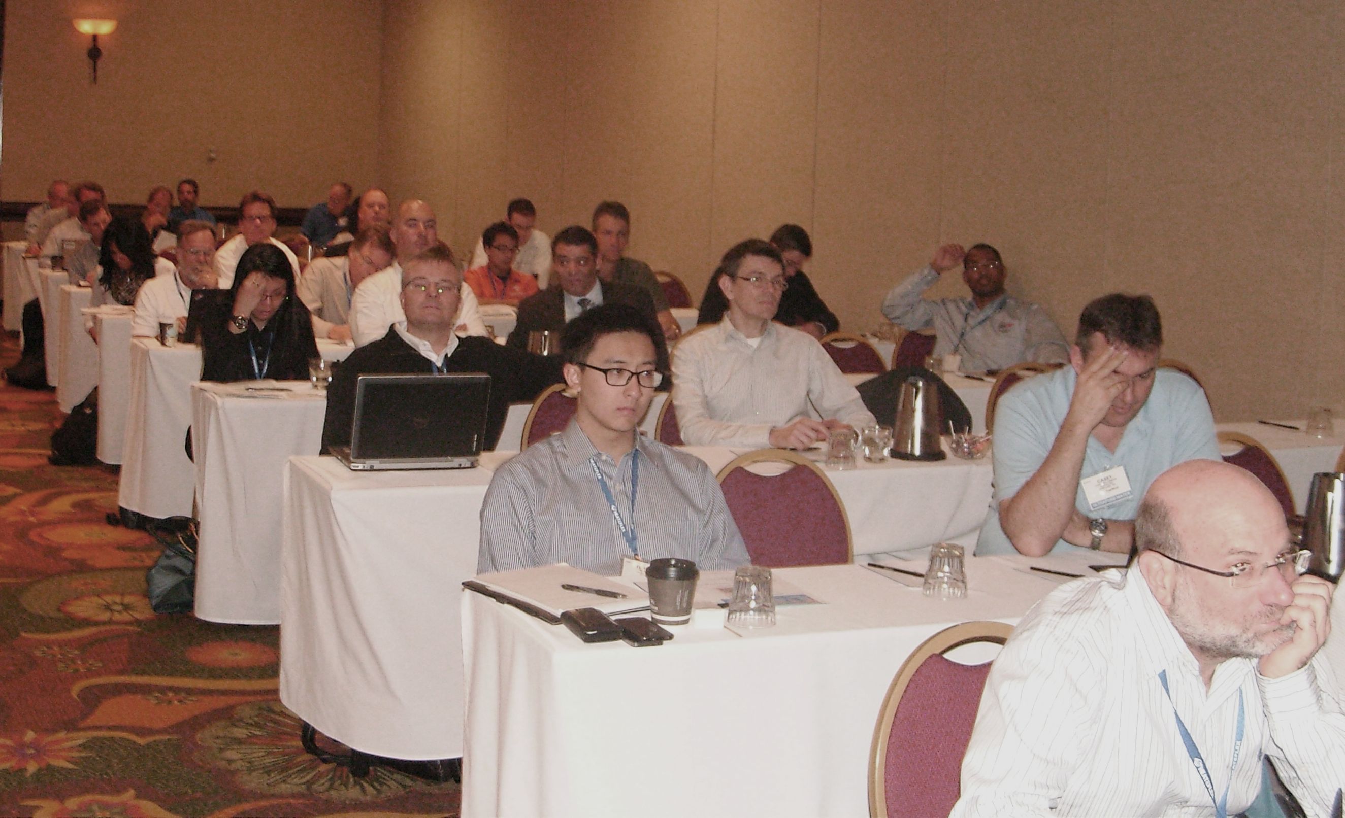
Conference speakers at this year's meeting will come from different aspects of semiconductor water treatment, and will include endusers, consultants, and engineers.
UPW Micro 2013 is a continuation of a series of focused conferences on semiconductor water that began in 1998. The last conference was conducted Nov. 13-14, 2012, in Phoenix. The May/June issue of ULTRAPURE WATER reviews the opening session at UPW Micro 2012, which had the overall theme of "Semiconductor Industry - Water Business Trends and Opportunities.
The opening speaker at UPW Micro 2012, Michael Corbett (1) of Linx Consulting in Mendon, Mass., noted that the industry segments include semiconductors, liquid crystal display (LCD), packaging, printed circuit boards (PCB), advanced batteries, and solar. As a part of his presentation, Mr. Corbett examined these topics: 450-mm wafers, adoption of extreme ultraviolet lithography (EUVL), and novel materials and devices.
The emergence of 450-mm wafers is expected to one day mean fewer new fabs are built. Even so, Mr. Corbett predicted that the economics of these fabs should expand the growth of the overall semiconductor market. He presented data showing estimates of worldwide wafer production through 2030. His data showed that the production of 200-mm wafers is already beginning to decline, while the manufacture of 450-mm wafers is expected to begin growing substantially after 2016, and by 2025 come to dominate the market. Meanwhile, the manufacture of the 300-mm size is expected to start declining substantially after 2020.
Mr. Corbett said that the emergence of 450-mm fabs will probably contribute to some slowing of the growth in the semiconductor water market since there will be fewer new fabs.
The coming use of the EUVL technology is expected to affect markets for photo-ancillaries, etch, and cleans, particularly spacers used with double patterning, Mr. Corbett said. The emergence of the EUVL will reduce the need for double patterning steps and will also help conserve water at wafer fabs. For example, in the manufacture of flash memory, a fab with the EUVL is predicted to use 1,500 million gallons per day (mgd) of water daily, while a plant using non-EUVL technology would need 2,000 mgd. For the manufacture of DRAM, the figure shows that non-EUVL would need more than 1,500 mgd, while a plant with EUVL technology should need to use just more than 1,000 mgd.
Abbas Rastegar, Ph.D., (2) of SEMATECH spoke on the particle defectivity challenges for sub-16 half-pitch (HP) nanometer (nm) devices. He said the following causes of defects are important for the microelectronics industry: environmental particles, contaminant particles impacting electrical performance, defects in starting materials, and printable defects from the lithography process. A killer particle on wafers reduces yields. These kinds of particles are determined by their size, type, and location. A critical concern arises when killer particle is on the mask because it is common for a mask to expose up to 100,000 wafers.
In the context of semiconductor water, Dr. Rastegar said that DI filtration with 10-nanometer (nm) filters has improved the mask cleaning yield. For example, particle measurement at a wet bench with a 50-nm filter followed by two 10-nm filters. This approach resulted in an average of 6 particles >25 nm per liter.
David Blackford, Ph.D., of FMT Inc., (3) discussed a report at UPW Micro 2012 on work by the ITRS (International Technology Roadmap for Semiconductors) and SEMI (Semiconductor Equipment and Materials International) toward current and future standards development. Other coauthors of this presentation were Slava Libman, Ph.D. of Balazs NanoAnalysis, Dan Wilcox of Spansion, and Marty Burkhart of Hi Pure Tech Inc.
The ITRS develops documents produced by semiconductor industry experts who are representative of the sponsoring organizations, which include the Semiconductor Industry Associations of the U.S., Europe, Japan, South Korea, and Taiwan. SEMI is a trade organization representing makers of equipment and materials used in the fabrication of semiconductor devices. SEMI acts as a clearinghouse for the development of standards and guidelines, and provides guidelines based on information from the ITRS.
Dr. Blackford said the ITRS' ultrapure water (UPW*) Roadmap is moving towards speciation and criticality and risk mitigation. He noted some changes include measurement of critical organics, and total organic carbon (TOC) measurement.
The full article in ULTRAPURE WATER is available at www.ultrapurewater.com. Visitors may also visit ULTRAPURE WATER's on-line bookstore. Books cover high-purity and industrial water treatment topics. CD Proceedings from past conferences may also be ordered.
References
1. Corbett, M. "Semiconductor Industry Trends and Opportunities", presentation at ULTRAPURE WATER Micro 2012, Phoenix, Ariz. (Nov. 13, 2012).
2, Rastegar, A. "Particle Defectivity Challenges for the Sub-16 nm HP Technology Node", presentation at ULTRAPURE WATER Micro 2012, Phoenix, Ariz. (Nov. 13, 2012).
3. Libman, S.; Blackford, D.; Wilcox, D.; Burkhart, M. "Semiconductor Technology Progress of UPW ITRS and SEMI Cooperation", presentation at ULTRAPURE WATER Micro 2012, Phoenix, Ariz. (Nov. 13, 2012).
Endnotes
*In the text, the term UPW refers to semiconductor-grade water produced in microelectronics facilities. Its quality parameters are defined under the International Technology Roadmap for Semiconductors (ITRS).
A CD Proceedings of the 2012 ULTRAPURE WATER Micro conference in Phoenix is available and may be ordered from the Tall Oaks Publishing Inc. web site at www.talloaks.com. The CD includes the three presentations highlighted in this article.
Related Media